
A chip that thinks in pulses
Photonic processors are often introduced through the enormous bandwidth of light, but their hardest problem is less glamorous: photons must arrive at the right detector with enough power to survive every splitter, modulator and waveguide on the way. A circuit can perform an elegant matrix multiplication on paper while becoming impractical once dozens of optical channels compete for the same finite laser budget. The constraint is especially sharp in a spiking neural network, where each neuron must emit pulses that are detected, weighted and converted into the next layer's activity.
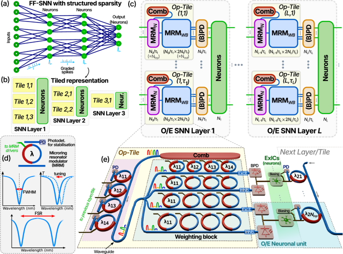
A study published on 23 October 2026 by Matěj Hejda, Aishwarya Natarajan, Chaerin Hong and colleagues presents an architecture called SEPhIA, a spiking electro-photonic integrated architecture. Its central idea is to replace the common one-laser-per-neuron arrangement with a shared multiwavelength source and compact silicon microring modulators. The authors examine not just whether a neuron can spike, but whether a network of such neurons remains useful after realistic crosstalk, optical loss, finite photodetector sensitivity and device variation are included. The result is a hardware-aware simulation of a two-layer classifier, not a fabricated, end-to-end optical neural-network chip [1].
The distinction matters because device demonstrations and system demonstrations answer different questions. An isolated microring may switch at high speed, and a laser may produce many wavelengths, yet a useful processor requires all of those components to function together. In the reported model, classification exceeds 90% on a restricted four-class benchmark. That performance establishes a plausible design point under the chosen assumptions, while leaving full-chip integration, thermal behavior and operation on more demanding tasks for later work.
Why the wavelengths must share the work
A frequency comb produces a set of discrete optical frequencies from one source. Each line can carry a separate signal, so a single waveguide transports several independent channels by wavelength-division multiplexing, or WDM. SEPhIA assigns optical channels to neurons through microring resonator modulators. Each ring selectively changes the transmission of a wavelength close to its resonance, allowing the electronic voltage spike to become an optical intensity pulse. The same waveguide can therefore carry the activity of many neurons without a separate laser cavity for each one.
A ring's resonance approximately satisfies the phase condition where is its circumference, is the effective index, and is an integer azimuthal mode number. Applying voltage changes the carrier distribution and effective refractive index, shifting the resonance. For a small perturbation, , where is the group index. That electrical control turns a resonant optical filter into a programmable modulator.
The network is organized into optical tiles, each with its own comb source, neuronal modulators, wavelength-selective weight bank and balanced photodetection. Several tiles implement sparse blocks of a larger weight matrix. The architecture reduces the number of laser sources relative to a design with one laser per neuron, but it does not abolish the need for optical power: every comb line must still survive routing, weighting and conversion at a detector [1,3].
From a capacitor to an optical spike
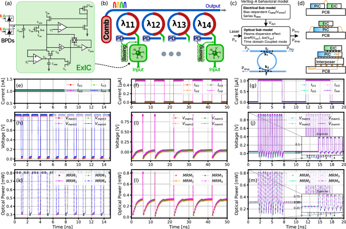
The spiking element is an electronic adaptive integrate-and-fire circuit coupled to a microring modulator. An electronic circuit accumulates an input-dependent voltage and generates an abrupt event after reaching an effective threshold. Its output drives a metal-oxide-semiconductor capacitor, or MOSCAP, integrated with the ring waveguide. The carrier redistribution modifies the optical resonance and transmits a spike on the corresponding wavelength. The circuit is therefore hybrid by design: electronic dynamics provide the nonlinear neuron, and optics carry the signals between neurons.
A simplified adaptive exponential integrate-and-fire model describes the membrane-like voltage and an adaptation current : When the voltage crosses a threshold, it is reset and the adaptation variable receives a discrete increment . The exponential term produces rapid spike initiation; the slow variable changes subsequent firing intervals. By tuning these parameters, the same circuit family produces tonic spiking, adaptation or bursts [1,4].
The authors couple a four-neuron electronic model to four microring modulators in Verilog-A and report simulated optical responses corresponding to those three firing regimes at approximately one billion spikes per second. This is a circuit-level transient simulation with physically informed device models, not a measured billion-spike-per-second operation of the full proposed network. Its value lies in showing that the intended CMOS dynamics and ring response are compatible in a joint time-domain description. The optical modulator's RC and carrier response are modeled as faster than the approximately nanosecond neuronal period, leaving the electronic neuron as the limiting stage in that model.
The resonance that can interfere with its neighbor
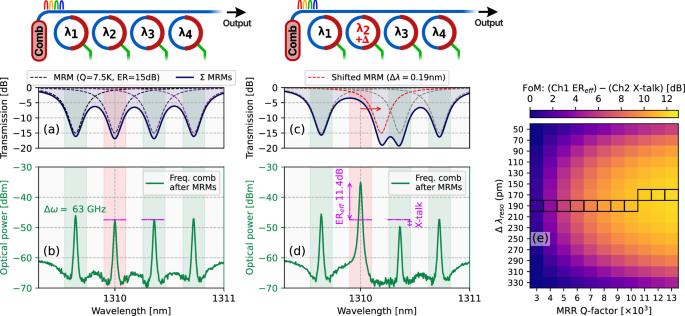
WDM is useful only if one wavelength can be modulated without unintentionally changing its neighbor. A ring resonance is not an infinitely narrow line. Its loaded quality factor, , relates the central optical frequency to the resonance linewidth . Increasing sharpens wavelength selectivity but also lengthens the photon storage time. A voltage-induced shift that is too small yields weak contrast; one that is too large approaches adjacent channels and creates crosstalk.
For a single resonance, a simple through-port model has the structure Here describes external coupling and internal loss. Real all-pass rings and fabricated coupling regions require their measured or modeled transfer functions, but the equation captures the central tradeoff: a resonance controls its own channel through detuning and affects nearby channels through its spectral tails.
At a nominal channel spacing of 63 GHz near 1310 nm, the study identifies an approximately 190-picometer ring-resonance shift as a favorable balance between effective extinction and adjacent-channel interference for its examined device settings. The optimum is not a universal constant: it depends on linewidth, channel spacing and the criterion used to balance extinction against crosstalk. Dense packing therefore requires system-level optimization rather than simply maximizing the number of wavelengths in a comb [1].
How an optical weight becomes a signed synapse
A photonic neural network must add both positive and negative weighted signals, although an optical detector directly measures nonnegative intensity. SEPhIA uses separate excitatory and inhibitory optical paths that terminate at balanced photodetectors. Subtracting their photocurrents produces an effective signed weighted sum. The optical ring bank selects how much power each input wavelength contributes to each output, while the differential detector turns two nonnegative optical intensities into a signed electrical signal.
If the optical powers arriving at a balanced pair are and , the idealized difference current is where is responsivity and collects detector noise. This is a practical implementation of inhibitory weights, but its precision depends on matching, finite extinction, shot noise, thermal noise and gain stability. The design's analog electronic stage then integrates that current and generates a new spike train.
The trainable optical weights are encoded as bounded resonance shifts, not arbitrary floating-point coefficients. A representative parameterization is , with a sigmoid that confines the shift to the physical tuning range. Backpropagation through time can update these effective control parameters while the simulated photonic transfer functions remain inside the computational graph. The benefit is that learning compensates for modeled device behavior rather than pretending the optics implement exact ideal multiplications [1,3,5].

What the classifier actually demonstrated
The reported architecture contains two parallel 16-by-16 optical weight-bank tiles in its first layer and a 16-by-8 tile in its second layer, with 16 first-layer spiking neurons and four output neurons. The study trains on a rate-coded, four-class subset of Fashion-MNIST rather than on the full ten-class image-recognition task. A single reported run reaches 91.35% test accuracy. Under comparable conditions, the authors report 93.65% for a fully connected software spiking baseline and 92.97% for a structurally sparse software baseline [1].
Those comparisons are informative but narrow. The photonic model's deficit relative to the sparse baseline is approximately 1.6 percentage points in the cited run, reflecting its modeled device imperfections and network behavior. The authors also report greater than 90% accuracy for suitable parameter choices across repeated training runs. This is not a general benchmark against state-of-the-art vision systems, nor evidence that the photonic implementation is already faster or more energy-efficient than a measured electronic accelerator at equal accuracy.
The network uses 35 simulation timesteps for backpropagation through time and trains 660 parameters, most of which control ring-resonance shifts. Because each input image is converted to spikes, the task exercises event processing and optical weighting but does not yet establish superiority on native temporal streams. Such tasks may be a better eventual match to the hardware, provided the same circuit and optical-power assumptions remain valid [1,5].

Noise is part of the calculation
At the photodetector, photon arrivals fluctuate even for an ideal coherent optical source. A standard approximate current-noise model includes shot noise and Johnson noise: Over an effective bandwidth , the corresponding variances scale as under a consistent one-sided spectral-density convention. The first contribution grows with detected current, while the second persists as a floor set by temperature and load resistance. The model treats these fluctuations statistically during the spiking computation.
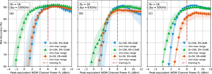
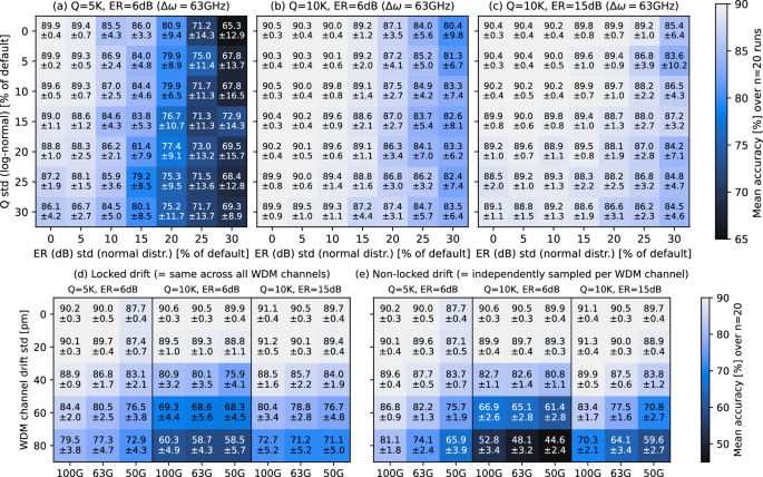
The study explores three comb-line spacings, 100, 63 and 50 GHz, together with ring quality factors of 5,000 or 10,000 and extinction ratios of 6 or 15 dB. A nominal 100 GHz spacing with and 15 dB extinction performs best among the reported configurations in the cited training comparison. Tighter spacing creates more opportunity for crosstalk, but the ranking of designs is not monotonic in any single device parameter. At 50 GHz spacing, a lower extinction ratio can perform better than a higher one under the tested conditions because resonance overlap and weight transfer functions change together.
A separate power sweep shows that accuracy can degrade both when individual comb lines become too weak and when operating far above the training power introduces model-dependent nonlinearities. More optical power is therefore not a free solution to poor signal-to-noise ratio. A robust architecture must operate within a range where detector statistics, ring tuning, electronic gain and the learned weights remain mutually consistent [1].
Fabrication errors and the advantage of common drift
Even rings drawn identically in a photonic layout acquire different resonance linewidths and coupling strengths after fabrication. Sidewall roughness, gap variations and local index changes can alter quality factor and extinction ratio. SEPhIA evaluates random component variation using Monte Carlo simulations, sampling up to 30% relative standard deviations for selected ring parameters. The resulting accuracy maps show that some device settings are substantially more sensitive than others; high nominal quality factor is not a guarantee of immunity to every kind of fabrication error.
The paper also distinguishes two types of laser drift. In a shared frequency comb, its channels may move together, preserving their relative spacing. In an array of separate lasers, each wavelength can drift independently. The simulations find that the common-drift case is more tolerant, plausibly because correlated changes can partly cancel at balanced detectors. The comparison uses wavelength-shift distributions of roughly 20 to 80 picometers around the 1310 nm operating band.
This is a system-level reason to share a light source beyond saving area. A common source can introduce correlations that make calibration simpler, although it also creates shared failure modes and common-mode intensity fluctuations. The reported analysis does not include every thermal or aging mechanism, and it assumes that the trained network is evaluated without retraining for the sampled fabrication variations [1].
The arithmetic of the optical power budget
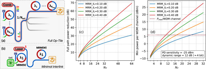
The clearest limit on tile size comes from multiplying modest component losses. A wavelength travels past neuronal rings, is split among output paths and passes through a weighting bank before detection. For a tile with input channels, output paths and a per-ring insertion loss expressed in decibels, an idealized lower bound on attenuation is The logarithmic term is the unavoidable penalty of passive splitting; the linear term counts the accumulated ring losses. Waveguide propagation, connectors and additional components would make the actual loss larger.
For a square tile with 16 channels and an assumed 0.2 dB insertion loss per ring, the model gives approximately 18.4 dB of minimum attenuation before other losses. That is a power ratio of about 69 to one. The estimate clarifies why adding channels eventually defeats the apparent economy of a shared laser: the same comb power must feed more branches while the optical signal crosses more resonant elements.
A second bound comes from spectral capacity. If the ring's free spectral range is about 1.306 THz and comb lines are separated by 100 GHz, only roughly 13 resonance positions fit within one free spectral range without additional wavelength management. Smaller spacing admits more channels but aggravates crosstalk. The paper therefore treats a tile size near 16 as a representative compromise, with the optical-power estimate and the frequency-spacing estimate imposing distinct restrictions [1,6].
Energy per spike needs a denominator
The electronic neuron is modeled as consuming approximately 4.586 microwatts under representative conditions, including a 10-femtofarad modulator load. That number is much smaller than the optical source contribution used for a full network tile. The authors estimate a representative optical channel power near 2.5 milliwatts to sustain the chosen operating point. Adding electronic and optical terms gives approximately 2.516 milliwatts per neuron-channel equivalent, or 2.516 picojoules per spike when divided by an assumed continuous one-gigaspike-per-second rate.
This ratio is not a measured wall-plug energy per useful inference. It excludes or idealizes several system costs, including some optical losses, packaging, laser-driver overhead and cooling, and the assumed spike rate is not necessarily the average rate of a sparse real workload. The same analysis considers a minimal two-ring interlink and obtains an illustrative 44 femtojoules per spike at the same assumed rate. These figures describe different optical paths and cannot be substituted for one another.
The useful question for photonic computing is therefore not whether light moves faster than electrons in a wire. It is whether a particular workload benefits from parallel optical transport after all conversion, amplification, detection, control and static-power costs are counted. Microring-based WDM creates a promising physical architecture, but its energy advantage remains contingent on integrated hardware and workload-level measurements [1,2,7].
What an integrated demonstration must resolve
A complete experiment would need fabricated rings with measured tuning efficiencies, a stable multiwavelength source, balanced photodetectors, CMOS spiking circuits and enough calibration control to maintain the learned weights. The paper combines experimentally motivated device parameters with circuit and architecture simulations, which is a substantial design exercise but not the same as demonstrating the entire signal chain on a chip. Thermal crosstalk among the photonic devices is not included in the reported simulator. Laser-to-laser variability, calibration energy, optical packaging and realistic application throughput also remain central questions.
The model's strongest conclusion is that architectural choices determine whether favorable device physics survives scaling. Sparse tiles limit the number of components that each optical signal traverses. Shared combs reduce the laser count and correlate wavelength drift. Balanced detection implements signed weights without requiring negative optical intensity. Hardware-aware training accounts for resonance shapes, losses and noise rather than hiding them inside an idealized matrix operation. None of these decisions alone solves the power budget, but together they define a concrete route for experimental testing.
A successful next-generation chip would be evaluated with measured energy per correctly classified event, latency, calibration frequency and accuracy on native temporal data. It would also need to show how performance changes as the number of tiles grows. The most important lesson from this 2026 work is that photonic spiking networks become scientifically interesting precisely when their optical constraints are treated as part of the computation, not as an afterthought.
References
- M. Hejda, A. Natarajan, C. Hong et al., “SEPhIA: spiking electro-photonic integrated tiled architecture leveraging multi-wavelength lasers for scalable optical neuromorphic computing,” npj Unconventional Computing 3, 56 (2026). https://doi.org/10.1038/s44335-026-00102-3.
- P. L. McMahon, “The physics of optical computing,” Nature Reviews Physics 5, 717–734 (2023). https://doi.org/10.1038/s42254-023-00645-5.
- A. N. Tait, T. Ferreira de Lima, E. Zhou et al., “Neuromorphic photonic networks using silicon photonic weight banks,” Scientific Reports 7, 7430 (2017). https://doi.org/10.1038/s41598-017-07754-z.
- R. Brette and W. Gerstner, “Adaptive exponential integrate-and-fire model as an effective description of neuronal activity,” Journal of Neurophysiology 94, 3637–3642 (2005). https://doi.org/10.1152/jn.00686.2005.
- J. K. Eshraghian et al., “Training spiking neural networks using lessons from deep learning,” Proceedings of the IEEE 111, 1016–1054 (2023). https://doi.org/10.1109/JPROC.2023.3308088.
- M. Buyalo, A. Gubenko, S. Mikhrin et al., “Efficient, high-power, narrow-linewidth, continuous-wave quantum-dot semiconductor comb laser,” Scientific Reports 14, 4197 (2024). https://doi.org/10.1038/s41598-024-53609-9.
- W.-C. Hsu, N. Nujhat, B. Kupp et al., “Sub-volt high-speed silicon MOSCAP microring modulator driven by high-mobility conductive oxide,” Nature Communications 15, 826 (2024). https://doi.org/10.1038/s41467-024-45130-4.
- B. Tossoun et al., “High-speed and energy-efficient non-volatile silicon photonic memory based on heterogeneously integrated memresonator,” Nature Communications 15, 551 (2024). https://doi.org/10.1038/s41467-024-44773-7.
- G. Indiveri et al., “Neuromorphic silicon neuron circuits,” Frontiers in Neuroscience 5, 73 (2011). https://doi.org/10.3389/fnins.2011.00073.
- D. A. B. Miller, “Attojoule optoelectronics for low-energy information processing and communications,” Journal of Lightwave Technology 35, 346–396 (2017). https://doi.org/10.1109/JLT.2017.2647779.