
When a channel remembers the voltage
A nanometre-wide channel filled with salt water can respond differently to the same applied voltage depending on what happened a few seconds earlier. Such a device is called a fluidic memristor: its conductance depends on a changing internal state, so a sweep of current against voltage traces a loop rather than a single-valued curve. For years, the microscopic state responsible for this behavior in two-dimensional slits has been debated. Proposed explanations include ion association, surface adsorption, concentration polarization and electrochemical changes. Many are plausible because ions near atomically smooth walls behave differently from ions in an ordinary beaker [2–5].
A study published on 27 October 2026 supplies unusually direct evidence for a different ingredient. Kalluvadi Veetil Saurav, Nathan Ronceray and collaborators measured ionic currents while simultaneously imaging the walls of layered nanochannels. They found that tiny liquid-filled blisters form and recede as the bias changes. The opening of these blisters increases the space available for ion transport; the delayed mechanical response generates electrical hysteresis [1]. The work examines fourteen devices, including nine used for a systematic classification of fifty individual blisters. Its contribution is to link local structural motion to the measured current in the same operating device, rather than infer a microscopic mechanism from an electrical curve alone.
The implication reaches beyond one particular memristor. At molecular dimensions, a channel's boundaries are active parts of the transport problem. Pressure, adhesion, surface charge and ionic redistribution can collectively determine the electrical response. Understanding the device therefore requires mechanics and electrokinetics to be treated as one coupled system.
Building an ångström-scale fluidic circuit
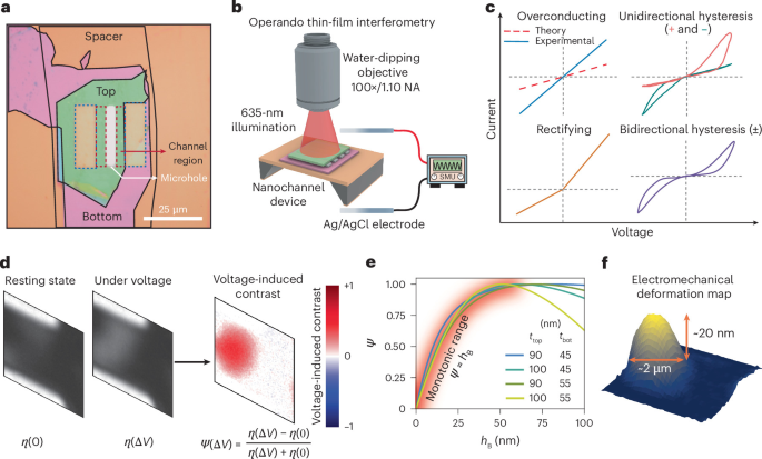
The channels consist of a layered stack assembled from hexagonal boron nitride, graphene spacers and another boron nitride sheet. The graphene spacer defines the nominal height of the water-filled slit with atomic-layer precision, while the boron nitride sheets form its ceiling and floor. The structure sits on a free-standing silicon-nitride membrane with a micrometre-scale aperture, and a second opening defines a channel length of approximately five micrometres [1]. The devices can be observed optically through the transparent layers while electrolyte is driven between reservoirs by silver/silver-chloride electrodes.
This geometry is a descendant of van der Waals capillaries in which atomically flat crystals act as walls and atomically thin spacers set their separation [6]. It offers excellent control over nominal confinement, but the interfaces are not guaranteed to remain perfectly bonded. Small patches can detach, allowing liquid to enter between sheets. A blister with a height of only a few nanometres may be mechanically modest yet electrically decisive because it changes the cross-sectional area of a channel that was initially only a few atomic layers high.
The experiment used potassium-chloride solutions over a wide concentration range and also examined other electrolytes. Sinusoidal voltage sweeps were synchronized with optical images, permitting direct comparison of electrical conductance and the shape of individual regions of the stack. Some channels behaved nearly ohmically, some rectified current, and others displayed pronounced hysteresis. That variety was a clue: a single idealized, rigid channel model was unlikely to capture the entire population [1].
The electrical signature of a hidden mechanical coordinate
A resistor with fixed conductance obeys an instantaneous relation between current and voltage. A memristive system instead contains one or more evolving internal coordinates. A useful phenomenological model is where the state variable can represent a blister height, area or adhesion configuration. This equation alone does not identify the physics of the memory; almost any slow internal process can generate a hysteretic loop. The experiment asks which state variable can actually be observed and correlated with the current.
For a narrow slit of width , length , conductivity and effective height , a simple bulk-conduction estimate is . This scaling is not a complete theory of surface-dominated ionic transport. It does show why a small local change in can have a large effect when the starting height is extremely small. The actual device contains multiple current paths and potentially several blisters, so the total conductance is governed by their network geometry as well as the height of each opening.
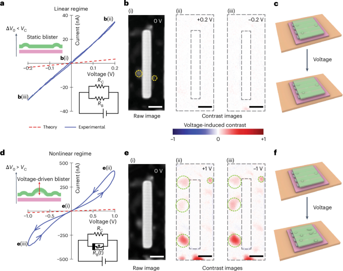
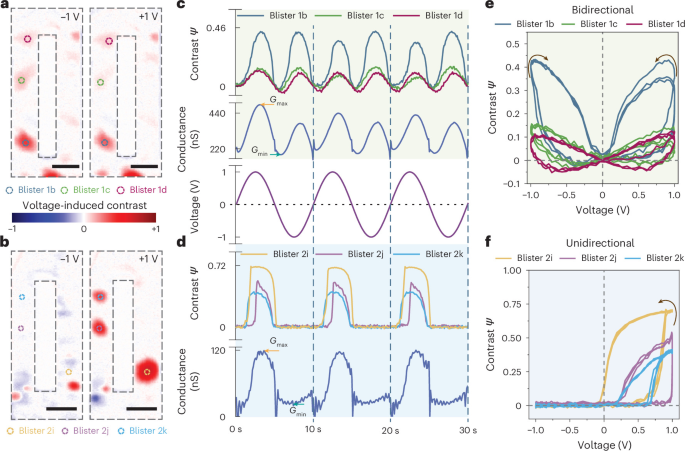
At a voltage amplitude of approximately 0.2 V, one measured channel showed an almost linear current response without voltage-dependent blistering. At a 1 V amplitude, the same channel developed hysteresis at the same time that its walls began to deform. The comparison isolates a threshold-like structural transition that accompanies the nonlinear electrical response. The reported onset depends on device and conditions; it should not be interpreted as a universal switching voltage for all nanofluidic systems [1].
Turning reflected light into a map of a nanometre blister
Ordinary optical microscopy cannot resolve a five-nanometre object by its lateral shape. The investigators instead exploit interference among light reflected at the interfaces of the layered stack. Changing the thickness of a liquid pocket changes optical path lengths and hence the measured reflectance. At each image pixel, they compare the intensity at applied voltage with the zero-bias intensity, defining a voltage-induced contrast Here is the recorded reflected-light intensity. A transfer-matrix optical calculation connects this dimensionless contrast to an estimated blister height for the measured layer thicknesses [1].
Crucially, contrast is a more direct observable than height. Conversion from one to the other depends on the thickness and refractive index of the stack, and those parameters have uncertainties. The paper therefore relies primarily on measured contrast for comparisons and treats inferred heights as approximate. Depending on geometry, blister formation can even produce contrast of opposite sign. A darkening region is not automatically evidence of a closing channel; the optical model must be calibrated for the particular stack.
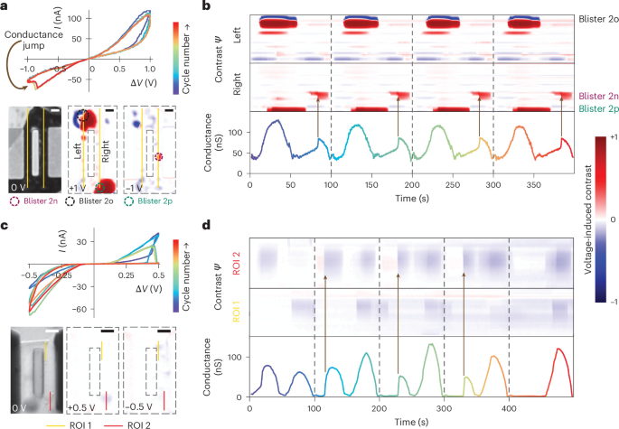
The technique also has a valuable temporal dimension. A kymograph records contrast along a chosen line over time, turning the movement of a blister edge into a trajectory that can be compared with the electrical signal. In one device, a reproducible conductance jump of about 50% in less than a second occurred near a negative bias of 0.7 V. The optical trace identified the local blister whose abrupt change coincided with that jump. In another, two separate responsive regions explained an evolving sequence of current jumps across successive cycles. These are substantially stronger correlations than a static before-and-after image could provide [1].
Two kinds of blister, two kinds of electrical memory
The images divide voltage-responsive blisters into two broad classes. Some expand under either polarity of the applied voltage: their response is bidirectional, approximately even in voltage. Others expand predominantly under one polarity and collapse under the opposite polarity: their response is unidirectional. This classification is based on the mechanical signal itself, not merely the direction of the current–voltage loop. It allows the same device to contain several local mechanisms that contribute differently to its total conductance.
For example, one channel displayed blisters that expanded under both positive and negative 1 V excitation, while a second showed growth principally at positive voltage. The corresponding conductance traces followed the same distinction. The authors also found mixed devices containing both response types. Their interpretation is that two physical pressure sources act on the flexible walls: osmotic pressure generated by ionic concentration polarization, and an electrostatic force acting on charged interfaces [1]. Those mechanisms make different predictions for the voltage parity of deformation.
The experiments also clarify the meaning of memory retention. Many blisters are volatile: they return to their initial shape when the voltage passes through zero. A subset remains partially deformed after the bias is removed, particularly during slow cycles. This structural persistence gives a physical candidate for a retained conductance state. It is not evidence that every channel provides stable nonvolatile storage, nor that the reported retention times are sufficient for commercial memory devices.
Why nominally identical devices disagree
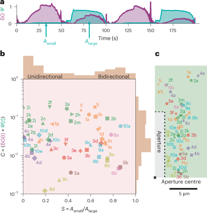
A major challenge in nanofluidic electronics is device-to-device variability. Small changes in adhesion, local contamination, channel geometry and surface charge can change when a blister nucleates, where it forms and whether it opens a useful ionic path. The new measurements make this variability spatially visible. Across nine devices, the team analyzed fifty blisters and extracted two descriptive quantities: a symmetry ratio , comparing integrated contrast over opposite half-cycles, and a contrast–conductance correlation [1].
Values indicate strongly one-sided deformation, whereas identifies approximately bidirectional motion. The correlation measures how closely an individual blister's optical signal follows the normalized conductance change. A blister can be mechanically active but electrically unimportant if it does not open a path that carries substantial current. Conversely, one strategically located blister can dominate the device. The fifty observed sites cluster into the two symmetry classes but show a broad distribution of conductance correlations.
One measured device reached an on/off conductance ratio near fifty, yet its response evolved irreversibly over four voltage cycles. This illustrates both the opportunity and the problem: a large switching ratio is useful only if the underlying structural state can be reproduced and controlled. Earlier work demonstrated that intentionally asymmetric nanofluidic channels can support reversible blister-based logic elements [2]. The new spatially resolved results show why engineering the nucleation site and adhesion landscape may matter as much as optimizing the electrolyte itself.
The mechanics of peeling an atomically thin wall
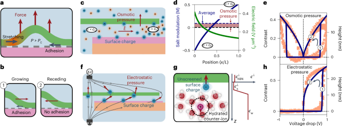
To lift a sheet away from its substrate, the liquid pressure must pay two energetic costs. It must stretch the elastic wall and overcome adhesion between adjacent surfaces. The authors analyze a blister with characteristic radius , layer thickness , in-plane Young's modulus , and effective adhesion energy per area . A simplified pressure threshold obtained from the elastic and adhesive energy balance is The expression describes the onset of detachment within the model's geometry and assumptions, not a universal failure pressure for every two-dimensional material [1,7].
Once a blister has opened and adhesion no longer constrains the moving area, the characteristic height scales as This cube-root law makes a clear physical prediction: doubling pressure does not double height. It also highlights how strongly the response depends on blister radius. The observed lateral radii are typically around one to a few micrometres, although the height changes are nanometric.
The mechanical barrier creates hysteresis naturally. Opening a new patch requires overcoming adhesion, but closing an already detached patch can follow a different energy path. This is why a pressure cycle can leave a transient structural memory even if the instantaneous pressure depends simply on the applied voltage. The fitted effective adhesion values are much lower than the strongest adhesion reported for pristine dry interfaces. The authors discuss interfacial residues and fluid-dependent interface evolution as possible reasons. The precise microscopic adhesion landscape remains a material-specific quantity to determine, not a universal constant.
Osmotic pressure: a response even in voltage
The first proposed driving mechanism begins with surface charge. A charged slit preferentially transports counterions; an applied field redistributes salt along its length. The resulting concentration polarization produces regions of enrichment and depletion. The pressure exerted by the enriched solution can lift a flexible wall. In the paper's simplified electrokinetic model, the osmotic contribution takes the form where is surface charge density, is channel height, and is the Dukhin number in the model's concentration convention [1,8].
The most informative feature is the square of the voltage. Reversing the electric field reverses the direction of ion migration, but it does not reverse the sign of the model's mean osmotic overpressure. Consequently, this mechanism can expand a blister at both voltage polarities. Combining the pressure scaling with the elastic height law gives above the detachment threshold. Using representative parameters, the model predicts pressures of order four bar, enough to drive the observed deformation when effective adhesion is sufficiently low.
These predictions require care at very high concentrations, where dilute-solution approximations may fail, and at rapidly varying biases, where the salt profile has not reached its assumed state. The experiments support the model through the observed parity and approximate height scaling; they do not directly image every microscopic ion distribution inside the slit.
Electrostatic pressure: a response odd in voltage
The second mechanism comes from electric field lines crossing the layers. Fixed surface charges experience a force normal to the wall, while mobile counterions in water are screened differently. In the simplest representation, the pressure is where is the local normal electric field. Because the sign of reverses with the applied bias, this contribution can favor opening under one voltage polarity and closing under the other. With representative surface charge densities, the model predicts pressures of order three bar [1].
Combining a pressure proportional to with the cube-root elastic law gives for the opening polarity. The paper compares both predicted classes of contrast–voltage curves with representative experimental blisters. Their agreement supports the proposed division between osmotic and electrostatic forcing. It does not establish that every blister has only one source of pressure; real devices may contain mixed contributions, spatially varying charges and different interfaces that peel under opposite signs.
Frequency, volatility and the time required to move liquid
A memristive loop is also a dynamical measurement. The wall cannot deform instantaneously because fluid must enter or leave the blister, while elastic forces and interfacial adhesion oppose that motion. At slow driving frequencies, the structure has time to respond and the current–voltage loop can become large. At faster driving, the deformation amplitude and hysteresis area diminish. The measurements show this behavior over the tested low-frequency range, with a characteristic suppression above roughly 100 mHz in the model [1].
The observed response is therefore not equivalent to a fast electronic memory cell. A 100 mHz voltage cycle lasts ten seconds, orders of magnitude slower than switching in mature semiconductor memory. Previous asymmetric nanofluidic devices operated on second timescales and implemented small logic circuits, but their speeds remain far from solid-state processors [2]. The interest here lies in a distinct materials mechanism and its possible uses in low-speed, liquid-compatible signal processing, not in a demonstrated replacement for digital memory.
Frequency dependence provides a further mechanistic test. A purely instantaneous electrostatic conductance change would not produce the same lag and retention behavior as a fluid-filled cavity governed by adhesion and hydrodynamic filling. Varying waveform, salt concentration, pressure and temperature while imaging the wall could distinguish how much of the lag originates from liquid flow, ion redistribution or the mechanics of detachment.
What this changes about nanoscale transport
The experiments show why a rigid-boundary approximation can fail even when the material forming the wall is mechanically strong. Atomically thin crystals are exceptionally stiff in-plane, but a suspended region can still bend and peel because the total bending and adhesion energy depends on geometry. At the same time, electrokinetic models that reproduce an electrical curve may remain underdetermined: several microscopic state variables can generate similar hysteresis. Imaging the wall provides an independent observable with which to discriminate mechanisms [1,3,4].
The results do not invalidate ionic association or adsorption as mechanisms in other nanofluidic systems. In fact, earlier theoretical and experimental studies found long-lived ionic memory and proposed interfacial processes in related geometries [3,5]. The specific conclusion here is stronger and narrower: in the examined two-dimensional devices, voltage-responsive blisters explain the observed conductance nonlinearities, and their polarity and temporal behavior are consistent with two classes of electromechanical forcing.
The most immediate engineering task is reproducibility. Controlling surface chemistry, adhesion, wall thickness and channel layout could make blister positions more deterministic. Directly patterned weak-adhesion sites might create a defined switching element instead of relying on stochastic delamination. More demanding tests would measure switching endurance, retention distributions, write energy, cross-device variability and behavior under integrated electrical readout. A useful future experiment would independently measure the local pressure or ion concentration while imaging the same blister, tightening the link between the proposed driving force and the observed deformation.
At the molecular scale, information can be stored in geometry as well as in charge. A few nanometres of wall motion can redirect ions through an entire channel, while adhesion determines whether the channel remembers its previous state. The new measurements make that coupling visible, offering a more concrete physical foundation for designing nanofluidic memory.
References
- K. V. Saurav, N. Ronceray, B. Coquinot et al., “Direct imaging elucidates ionic memory in two-dimensional nanochannels,” Nature Materials (published 27 October 2026). doi:10.1038/s41563-026-02775-4.
- T. Emmerich, Y. Teng, N. Ronceray et al., “Nanofluidic logic with mechano–ionic memristive switches,” Nature Electronics 7, 271–278 (2024). doi:10.1038/s41928-024-01137-9.
- P. Robin, T. Emmerich, A. Ismail et al., “Long-term memory and synapse-like dynamics in two-dimensional nanofluidic channels,” Science 379, 161–167 (2023). doi:10.1126/science.adc9931.
- A. Ismail, G.-H. Nam, A. Lokhandwala et al., “Programmable memristors with two-dimensional nanofluidic channels,” Nature Communications 16, 7008 (2025). doi:10.1038/s41467-025-61649-6.
- P. Robin, N. Kavokine and L. Bocquet, “Modeling of emergent memory and voltage spiking in ionic transport through angström-scale slits,” Science 373, 687–691 (2021). Author manuscript.
- B. Radha, A. Esfandiar, F. C. Wang et al., “Molecular transport through capillaries made with atomic-scale precision,” Nature 538, 222–225 (2016). doi:10.1038/nature19363.
- N. Ronceray, M. Spina, V. H. Y. Chou et al., “Elastocapillarity-driven 2D nano-switches enable zeptoliter-scale liquid encapsulation,” Nature Communications 15, 185 (2024). doi:10.1038/s41467-023-44200-3.
- S. J. Kim, Y.-C. Wang, J. H. Lee, H. Jang and J. Han, “Concentration polarization and nonlinear electrokinetic flow near a nanofluidic channel,” Physical Review Letters 99, 044501 (2007). doi:10.1103/PhysRevLett.99.044501.
- L. Fumagalli, A. Esfandiar, R. Fabregas et al., “Anomalously low dielectric constant of confined water,” Science 360, 1339–1342 (2018). doi:10.1126/science.aat4191.
- K. V. Saurav et al., “Dataset of ‘Direct imaging elucidates ionic memory in two-dimensional nanochannels’,” figshare (2026). doi:10.6084/m9.figshare.33269229.